Make: Electronics (61 page)
Authors: Charles Platt

And while you’re thinking about this, see if you can figure out the inputs and output of three ANDs in the same configuration.
For a four-player game, you’ll also need two additional 555 timers, of course, and two more LEDs, and two more pushbuttons.
As for creating a schematic for the four-player game—I’m going to leave that to you. Begin by sketching a simplified version, just showing the logic symbols. Then convert that to a breadboard layout. And here’s a suggestion: pencil, paper, and an eraser can still be quicker, initially, than circuit-design software or graphic-design software, in my opinion.
Experiment 22: Flipping and Bouncing
I mentioned in the previous experiment that “bounce” from the buttons in the circuit wouldn’t be a problem, because the buttons were activating 555 timers that were wired in bistable, flip-flop mode. As soon as the timer receives the very first pulse, it flips into its new state and flops there, ignoring any additional noise in the circuit. So can we debounce a switch or a button using a flip-flop? And as some 74HCxx chips are available containing flip-flops, can we use them?
The answers are yes, and yes, although it’s not quite as simple as it sounds.
You will need:
- 74HC02 logic chip containing 4 NOR gates. 74HC00 logic chip containing 4 NAND gates. Quantity: 1 of each.
- SPDT switch. Quantity: 1.
- LEDs, low-current. Quantity: 2.
- 10K resistors and 1K resistors. Quantity: 2 of each.
Assemble the components on your breadboard, following the schematic shown in Figure 4-98. When you apply power (through your regulated 5-volt supply), one of the LEDs should be lit.
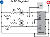
Figure 4-98.
A simple circuit to test the behavior of two NOR gates wired as a simple flip-flop that retains its state after an input pulse ceases.
Now I want you to do something odd. Please disconnect the SPDT switch by taking hold of the wire that connects the positive power supply to the pole of the switch, and pulling the end of the wire out of the breadboard. When you do this, you may be surprised to find that the LED remains lit.
Push the wire back into the breadboard, flip the switch, and the first LED should go out, while the other LED should become lit. Once again, pull out the wire, and once again, the LED should remain lit.
Here’s the take-home message:
- A flip-flop requires only an initial pulse.
- After that, it ignores its input.
How It Works
Two NOR gates or two NAND gates can function as a flip-flop:
- Use NOR gates when you have a positive input from a double-throw switch.
- Use NAND gates when you have a negative input from a double-throw switch.
Either way, you have to use a double-throw switch.
I’ve mentioned the double-throw switch three times (actually, four times if you count this sentence!) because for some strange reason, most introductory books fail to emphasize this point. When I first started learning electronics, I went crazy trying to understand how two NORs or two NANDs could debounce a simple SPST pushbutton—until finally I realized that they can’t. The reason is that when you power up the circuit, the NOR gates (or NAND gates) need to be told in which state they should begin. They need an initial orientation, which comes from the switch being in one state or the other. So it has to be a double-throw switch. (Now I’ve mentioned it five times.)
I’m using another simplified multiple-step schematic, Figure 4-99, to show the changes that occur as the switch flips to and fro with two NOR gates. To refresh your memory, I’ve also included a truth table showing the logical outputs from NOR gates for each combination of inputs.
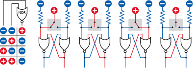
Figure 4-99.
Using two NOR gates in conjunction with a positive input through a SPDT switch, this sequence of four diagrams shows how a flip-flop circuit responds.
Suppose that the switch is turned to the left. It sends positive current to the lefthand side of the circuit, overwhelming the negative supply from the pull-down resistor, so we can be sure that the NOR gate on the left has one positive logical input. Because any positive logical input will make the NOR give a negative output (as shown in the truth table), the negative output crosses over to the righthand NOR, so that it now has two negative inputs, which make it give a positive output. This crosses back to the lefthand NOR gate. So, in this configuration everything is stable.
Now comes the clever part. Suppose that you move the switch so that it doesn’t touch either of its contacts. (Or suppose that the switch contacts are bouncing, and failing to make a good contact. Or suppose you disconnect the switch entirely.) Without a positive supply from the switch, the lefthand input of the left NOR gate goes from positive to negative, as a result of the pull-down resistor. But the righthand input of this gate is still positive, and one positive is all it takes to make the NOR maintain its negative output, so nothing changes. In other words, the circuit has “flopped” in this state.
Now if the switch turns fully to the right and supplies positive power to the righthand pin of the right NOR gate, quick as a flash, that NOR recognizes that it now has a positive logical input, so it changes its logical output to negative. That goes across to the other NOR gate, which now has two negative inputs, so its output goes positive, and runs back to the right NOR.
In this way, the output states of the two NOR gates change places. They flip, and then flop there, even if the switch breaks contact or is disconnected again. The second set of drawings in Figure 4-100 shows exactly the same logic, using a negatively powered switch and two NAND gates. You can use your 74HC00 chip, specified in the parts list for this experiment, to test this yourself.
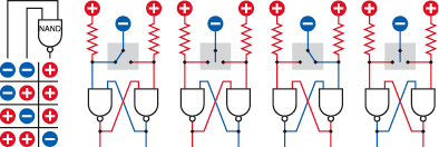
Figure 4-100.
The schematic from Figure 4-99 can be rewired with NAND gates and a negative switched input.
Both of these configurations are examples of a jam-type flip-flop, so called because the switch forces it to respond immediately, and jams it into that state. You can use this circuit anytime you need to debounce a switch (as long as it’s a double-throw switch).
A more sophisticated version is a clocked flip-flop, which requires you to set the state of each input first and then supply a clock pulse to make the flip-flop respond. The pulse has to be clean and precise, which means that if you supply it from a switch, the switch must be debounced—probably by using another jam-type flip-flop! Considerations of this type have made me reluctant to use clocked flip-flops in this book. They add a layer of complexity, which I prefer to avoid in an introductory text.
What if you want to debounce a single-throw button or switch? Well, you have a problem! One solution is to buy a special-purpose chip such as the 4490 “bounce eliminator,” which contains digital delay circuitry. A specific part number is the MC14490PG from On Semiconductor. This contains six circuits for six separate inputs, each with an internal pull-up resistor. It’s relatively expensive, however—more than 10 times the price of a 74HC02 containing NOR gates. Really, it may be simpler to use double-throw switches that are easily debounced as described previously.
Experiment 23: Nice Dice
This is the one experiment where I want you to use the 74LSxx generation of the TTL logic family, instead of the 74HCxx family of CMOS. Two reasons: first, I need to use the 7492 counter, which is unavailable in the HC family. And second, you should know the basic facts about the LS series of TTL chips, as they still crop up in circuits that you’ll find in electronics books and online.
In addition, you’ll learn about “open collector” TTL chips such as the 74LS06 inverter, which can be a convenient substitute for transistors when you want to deliver as much as 40mA of current.
The idea of this circuit is simple enough: run a 555 timer sending very fast pulses to a counter that counts in sixes, driving LEDs that are placed to imitate the spots on a die. (Note that the word “die” is the singular of “dice.”) The counter runs so fast, the die-spots become a blur. When the user presses a button, the counter stops arbitrarily, displaying an unpredictable spot pattern.
Dice simulations have been around for many, many years, and you can even buy kits online. But this one will do something more: it will also demonstrate the principles of binary code.
So, if you’re ready for the triple threat of TTL chips, open collectors, and binary, let’s begin.
You will need:
- 74LS92 counter such as SN74LS92N by Texas Instruments. Quantity: 1 if you want to create one die, 2 to make two dice.
- 74LS27 three-input NOR gate such as SN74LS27N by Texas Instruments. Quantity: 1.
- 555 timers. Quantity: 1 if you want to make one die, 2 to make two dice.
- Signal diodes, 1N4148 or similar. Quantity: 4, or 8 to make two dice.
Seeing Binary
The counter that we dealt with before was unusual, in that its outputs were designed to drive seven-segment numerals. A more common type has outputs that count in binary code.
The 74LS92 pinouts are shown in Figure 4-101. Plug the chip into your breadboard and make connections as shown in Figure 4-102. Initially, the 555 timer will drive the counter in slow-motion, at around 1 step per second. Figure 4-103 shows the actual components on a breadboard.
Note that the counter has unusual power inputs, on pins 5 and 10 instead of at the corners. Also four of its pins are completely unused, and do not connect with anything inside the chip. Therefore, you don’t need to attach any wire to them on the outside.
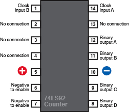
Figure 4-101.
The unusual pin assignments include four that have no connection of any kind inside the chip, and can be left unattached.